
PCB Layout Design
We provide design services in world wide used designing softwares. Tips also provide reverse engineering work to customers.
- Make outline as per customer requirement.
- Convert schematic to layout design.
- Put mounting hole as per customer requirement.
- Make cutout as per customer requirement.
- Make slot drill as per customer requirement.
- Make drill drawing.
- Make customer specific array/panelization.
- Design single ended /differential trace layout.
- Taken gerber 274X or other format output of design.
- Taken NC drill output of drill.
- Make fabrication drawing.
Tips provide some facilities for
- Design for manufacturability (DFM).
- Reverse engineering for single & double side board
- Design for Surface mount, through hole, mixed technology (BGA, PGA) & fine pitch components.
- Generate bill of material.
- Stack up creation of multilayers.
- Stencil layers for smd assembly.
- Make drill drawing.
PCB Design by TIPS
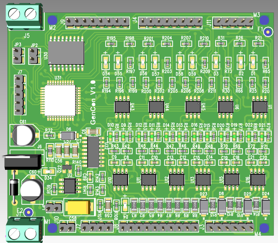
3D PRINTER CARD - 3D TOP VIEW
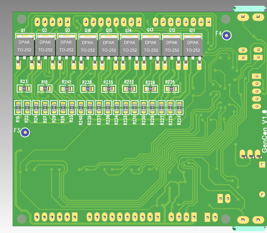
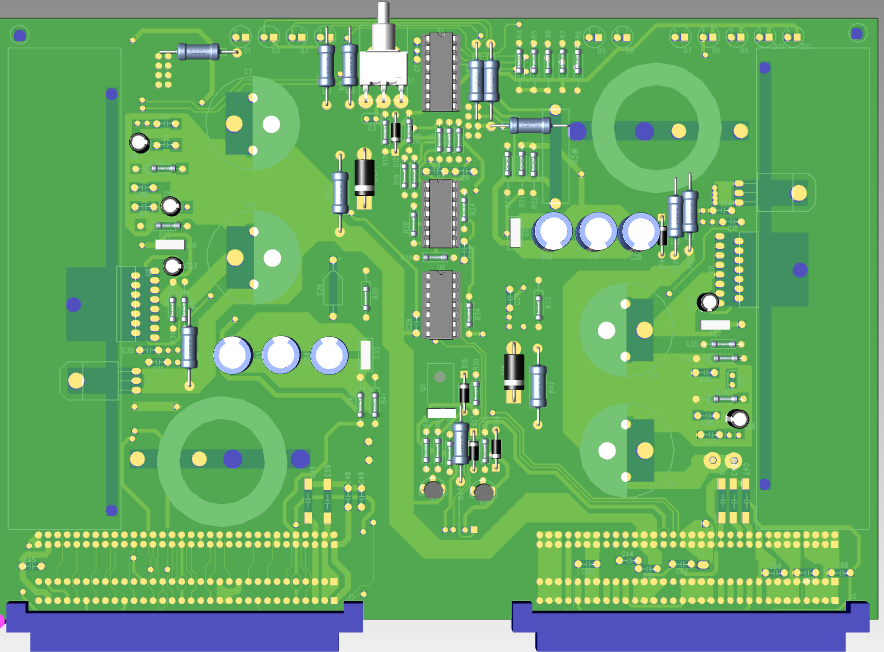
3D PRINTER CARD - 3D BOT VIEW
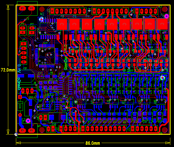
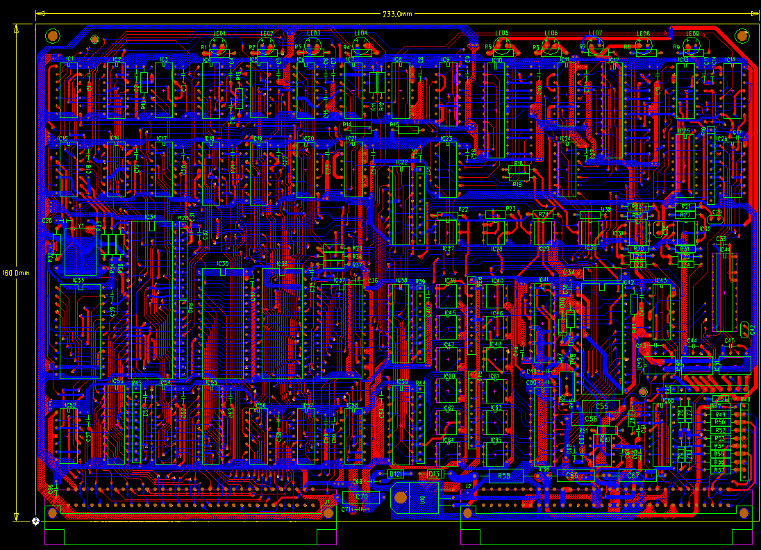
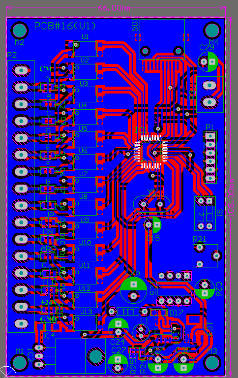
3D PRINTER CARD - LAYOUT
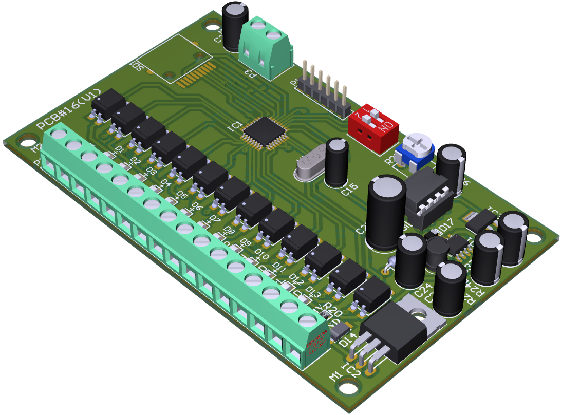
REVERSE ENGINEERING - 3D TOP VIEW
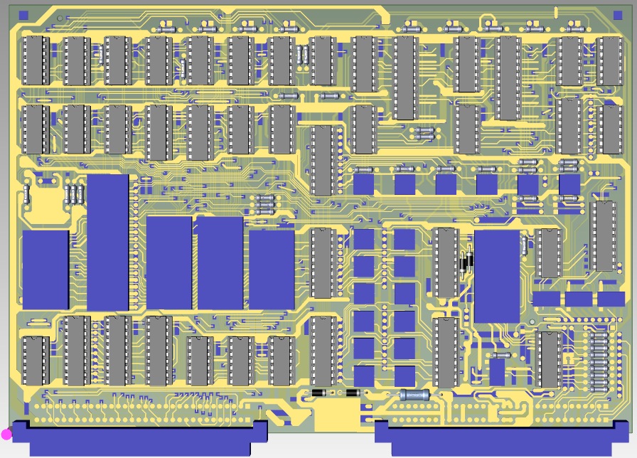
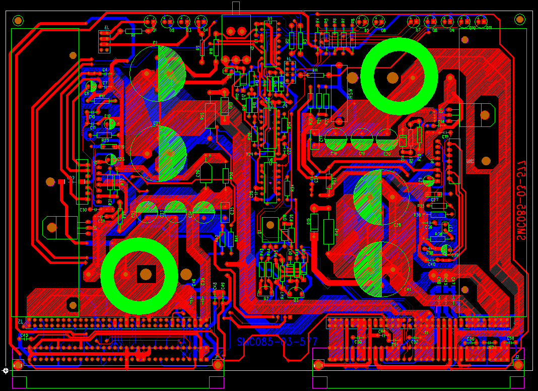
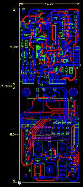
REVERSE ENGINEERING - LAYOUT
REVERSE ENGINEERING - 3D TOP VIEW
REVERSE ENGINEERING - LAYOUT
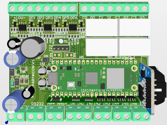
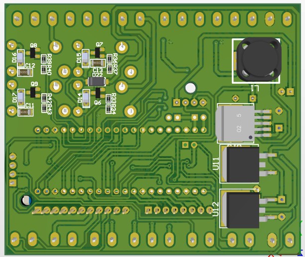
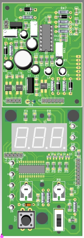
3D PRINTER DRIVER CARD-3D TOP VIEW
3D PRINTER DRIVER CARD-3D BOT VIEW
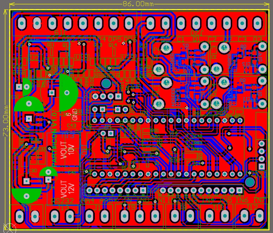
3D PRINTER DRIVER CARD-LAYOUT
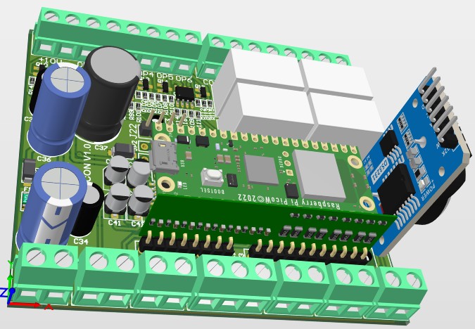
3D PRINTER DRIVER CARD-3D DEFAULT VIEW
ELEVATOR CARD - 3D TOP VIEW
ELEVATOR CARD - LAYOUT
DIGITAL EMCB DESIGN - 3D TOP VIEW
DIGITAL EMCB DESIGN - LAYOUT
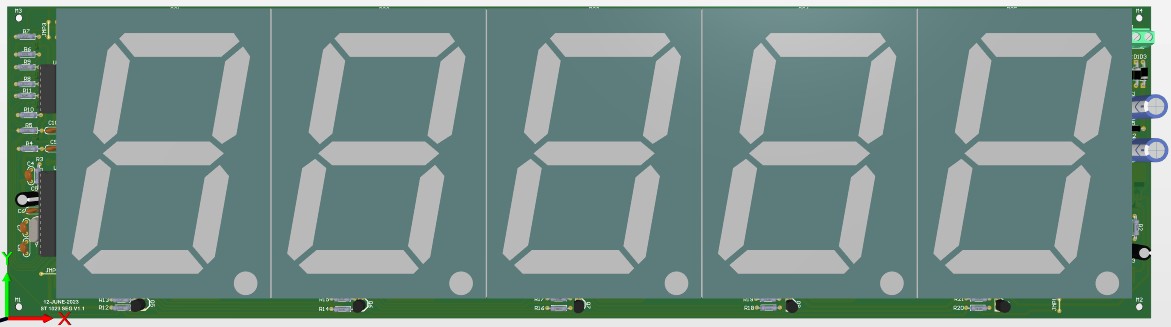
CRAIN LOAD DISPLAY-3D TOP VIEW
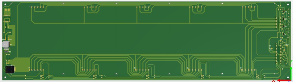
CRAIN LOAD DISPLAY-3D BOT VIEW
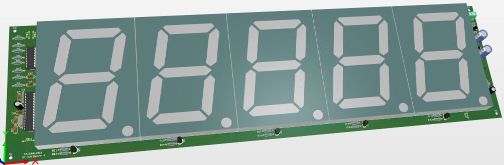
CRAIN LOAD DISPLAY-3D DEFAULT VIEW
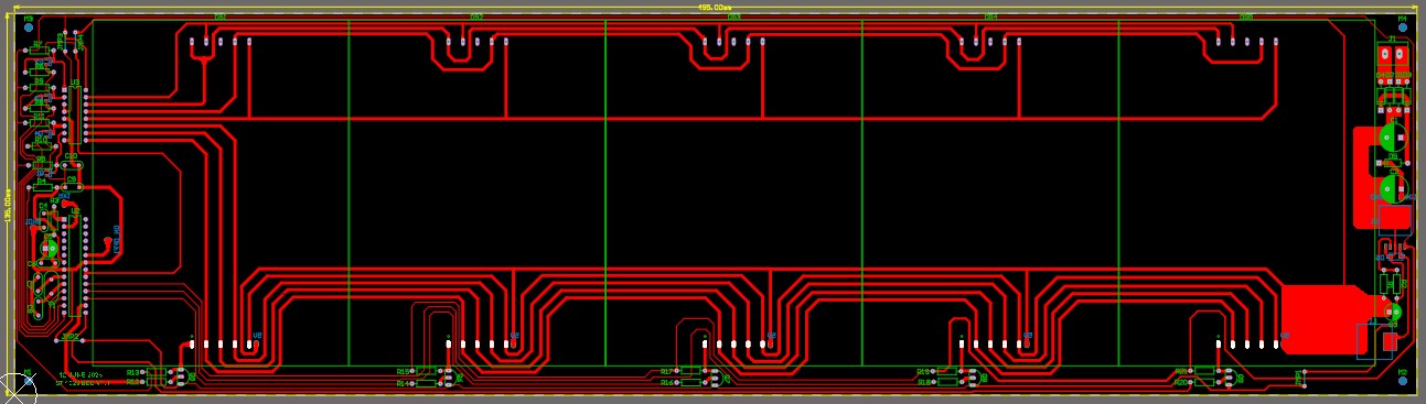
CRAIN LOAD DISPLAY-LAYOUT
CRAIN LOAD DOT MATRIX DISPLAY-3D TOP VIEW
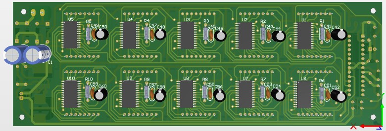
CRAIN LOAD DOT MATRIX DISPLAY-3D BOT VIEW
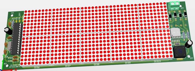
CRAIN LOAD DOT MATRIX DISPLAY-3D DEFAULT VIEW
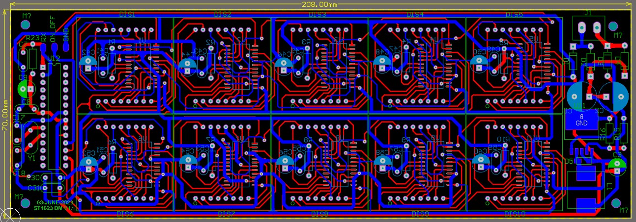
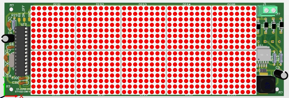
CRAIN LOAD DOT MATRIX DISPLAY-LAYOUT
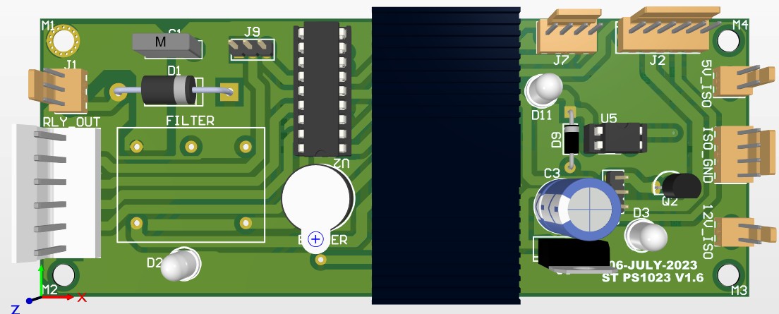
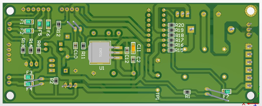
POWER SUPPLY-3D-TOP VIEW
POWER SUPPLY-3D-BOT VIEW
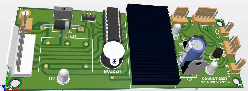
POWER SUPPLY-3D-DEFAULT VIEW
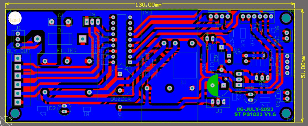
POWER SUPPLY-LAYOUT
Click on image to view Large Image / Gallery View